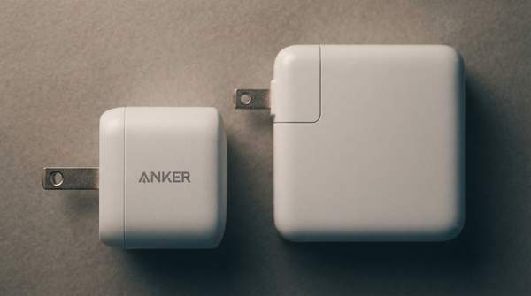
For any seasoned traveler, the ritual is familiar: the careful packing of a tangled nest of power bricks and cables, each dedicated to a specific device. For decades, the silicon-based chargers for our laptops, phones, and tablets have been a bulky, non-negotiable burden. The arrival of Gallium Nitride (GaN) technology has fundamentally altered this reality, offering chargers that deliver the same or even greater power from a dramatically smaller and lighter package. This transformation is not a simple feat of clever design but the direct result of GaN's superior properties as a semiconductor, allowing it to outperform the material that has defined electronics for generations.
At its core, GaN is a compound that conducts electricity far more efficiently than traditional silicon. This efficiency is the key to its revolutionary impact. When a charger converts AC power from a wall outlet to the DC power your devices need, inefficiency manifests as wasted energy, primarily in the form of heat. By generating significantly less heat, GaN allows engineers to design chargers with smaller, more densely packed components without the risk of overheating. The result is a new class of power adapter that is not only more portable but also cooler to the touch and more energy-efficient, making it an almost perfect solution for the modern traveler.
Understanding GaN: The Core Difference from Silicon
To appreciate the leap forward that Gallium Nitride represents, one must first understand the role of the semiconductor at the heart of every charger. These materials are the gatekeepers of electricity, precisely controlling the flow of current. For over half a century, silicon has been the undisputed workhorse of the electronics industry. It is abundant, reliable, and well-understood. However, silicon has inherent physical limitations, especially when it comes to managing high power in a small space. As our devices have become more power-hungry, the silicon-based chargers required to fuel them have remained stubbornly large.
Gallium Nitride enters as a challenger with a fundamentally different atomic structure that gives it a crucial advantage. This advantage is best quantified by a property known as the bandgap, which is the amount of energy required to make an electron in the material break free and conduct electricity. According to published lab measurements, GaN has a wide bandgap of 3.4 electron volts (eV), nearly triple the 1.1 eV bandgap of silicon. This seemingly abstract physical difference has profound, real-world consequences. A material with a wider bandgap can withstand much higher voltages and operate at higher temperatures before its electrical properties begin to break down.
For a power adapter, which must handle the full voltage from a wall outlet, this resilience is paramount. Because GaN can tolerate more electrical stress than silicon, the components built from it can be made significantly smaller while performing the same job, setting off a chain reaction of miniaturization throughout the charger's design.